ELEKTRONICA
- 1 januari 2013
- Reacties uitgeschakeld voor ELEKTRONICA
- in ELEKTRONICA
Objective
The objective of this work package is to increase knowledge of techniques for manufacturing 3D electronics and to realize applications for better and more efficient products and production processes.
Project activities
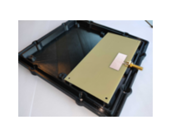
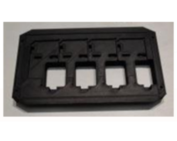
The technical scope of this work package includes various techniques, such as 'pure' 3D printing techniques, the combination of 3D printing with the placement of electrically conductive tracks and components in a separate process step, but also the 3-dimensional placement of tracks and components on plastic parts manufactured with injection molding technology. Also in scope is the deposition of metal on plastic parts for eg electromagnetic shielding.
Activities are aimed at acquiring knowledge of various techniques and ultimately combining them for application.
- Exploring the possibilities and limits of 3D electronics and testing them in test modules to map out the potential of 3D electronics and the associated manufacturing techniques. Examples of knowledge to be gained are knowledge of material properties, process properties, and process knowledge of the metallization of printed parts.
- Exploring applications for 3D electronics to create products and tools containing conductive traces and components, both on the surface and internally.
business case
Due to the ever increasing complexity of electronics in products and production processes, 3D electronics is a growth market. Various fields of application are important in this regard. The application of 3D electronics in the production of both small and larger product series makes it possible to achieve significant gains in, for example, material reduction, miniaturization, energy efficiency, robustness (due to better shielding from both weather influences and electromagnetic interference), and durability.
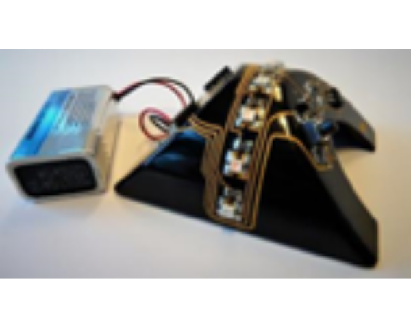
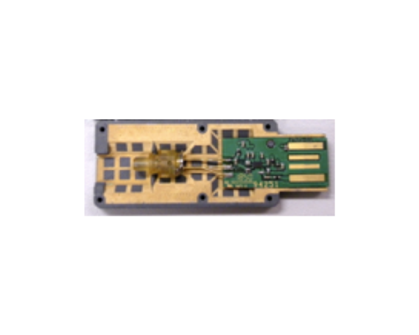
However, one-off production is also important, not only for the manufacture of unique (e.g. personalized) products, but also because it enables the development of 3D electronic products through experimentation and prototyping and thereby stimulates innovation. In addition, several production processes require the use of tools in which electronics and mechanics are integrated. An example of this is the test voltages used in the production of electronics, which are complex units consisting of a holder with cables, connectors, LEDs, with anti-static properties, and which could be largely replaced by a single part consisting of integrated mechanics and electronics (with conductive traces) in a single housing.
The feasibility is real. In the past 2-3 years it has been shown that metals on plastics offer many possibilities. The first successful steps towards the development of 3D electronics have been taken in two previous projects within the Northern Netherlands (part of the Region of Smart Factory and the Innovation Cluster Drachten). However, the roadmap is not yet complete and requires further knowledge development. Ultimately, the acquired knowledge enables us to better connect with the international market and to lead the way in this technology as a region within the Netherlands.
Philips, Variass and ASTRON work together in the work package, each with its own area of interest and focus, and sharing and disseminating knowledge together.